Infineon Runs 300-mm Silicon Carbide Wafers Through a Full-Scale Fab
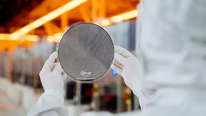
Infineon Technologies AG said on 9 November 2026 that it has processed 300-millimeter (300-mm) silicon carbide (SiC) wafers into functional power devices at its fab in Villach, Austria. The company states it is the first to do this in a full-scale semiconductor fab environment.
According to Infineon, the devices were made on existing silicon manufacturing equipment. The company says chip production on 300-mm wafers yields 2.3 times more chips per wafer than on 200-mm wafers. The announcement also says Infineon has proven the feasibility of its Cold Split technology with 300-mm SiC at its Dresden, Germany site. Cold Split separates wafers from a SiC boule (a cylindrical single-crystal ingot), which Infineon says involves less material loss and substantially reduced processing time than conventional wire sawing.
Infineon will show its first processed 300-mm SiC wafer publicly at the electronica trade show in Munich, starting 10 November 2026. The wafer display is a scheduled presentation, and the announcement does not describe any commercial shipment of 300-mm SiC products.
The 300-mm work builds on the company's 200-mm SiC program. In February 2025, Infineon said it had reached a milestone on its 200-mm SiC roadmap, with product roll-out to customers beginning. Infineon and Wolfspeed have also expanded and extended their long-term SiC wafer supply agreement to cover 200-mm wafers in addition to the existing 150-mm supply.
The company's wider wide-bandgap roadmap includes gallium nitride (GaN), a material used in high-efficiency power switching. On 27 October 2026, Infineon announced an investment of approximately €1.1 billion in a high-volume GaN power semiconductor facility on 300-mm wafers in Villach. Earlier, in September 2024, Infineon said it had produced GaN chips on 300-mm wafers, which it described as a world first, and it announced plans to present 300-mm GaN wafers at electronica that November.
In my view, the yield multiplier is the figure to track. A per-wafer gain of 2.3 times is a geometric statement about die count, but cost per good die depends on how many of those dies pass test at volume. That question belongs to the ramp, not to the milestone.
The broader context here is a material problem. SiC is hard to slice and expensive to process, and much of the cost sits in substrate and wafer handling rather than in the active device. If larger wafers can run on tools already in use for silicon, and if a separation method cuts both material loss and cycle time, the cost structure of SiC power devices changes at the margin. Whether that change arrives at the scale power-conversion customers need will depend on yield, qualification and capacity decisions that will unfold over the next several years.
For fab engineers, the practical signal is that the 300-mm transition is moving from pilot lines toward production-compatible flows for SiC, the same path silicon took in the previous decade. The next public data points will be the electronica demonstration and any follow-up disclosures on yield, qualification timelines and volume plans.