Google's Next-Gen AI Chip "Frozen v2" Targets Up to 10x Efficiency Gains
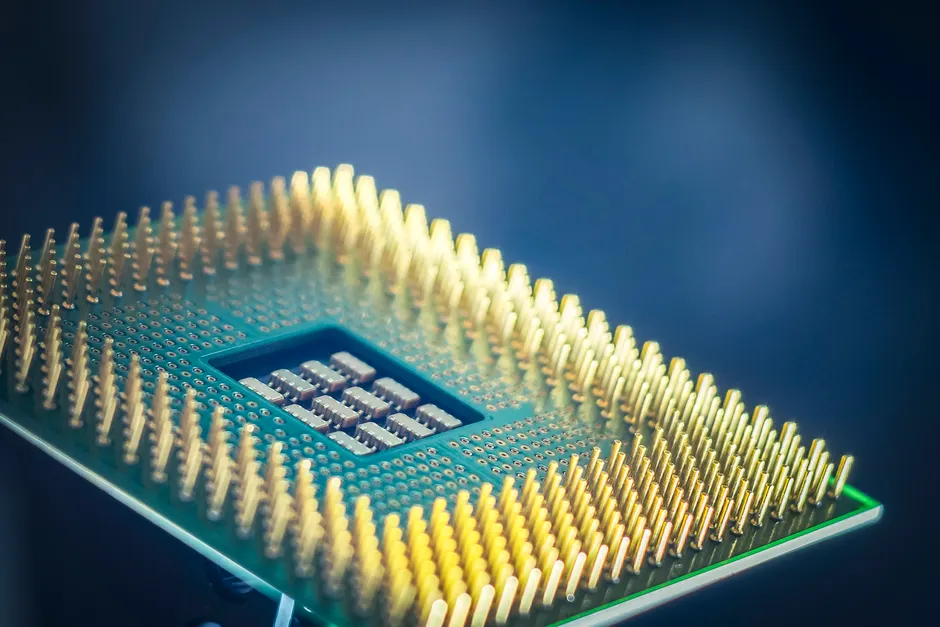
Alphabet is developing a new custom server chip internally called "Frozen v2" that could deliver six to ten times the inference efficiency of Google's current AI silicon, according to a report first published by The Information on July 20, 2026. Reuters independently corroborated the efficiency figure, citing the same tokens-per-unit-of-power metric (Reuters).
Inference is the process of a trained AI model actually answering queries or generating output, as opposed to training, which is the initial learning phase. The metric in question — how many tokens (units of text output) a chip can produce per unit of electricity — directly affects how much it costs to run a large AI model in daily use.
The chip is reportedly slated for release sometime in 2028. According to CNBC, Frozen v2 would embed parts of Gemini's architecture directly into the silicon, a design choice that shifts work from software to fixed-function hardware in pursuit of throughput and energy savings. In other words, rather than relying on general-purpose chips that can run many different models, Google would bake some of Gemini's specific design into the physical circuitry of the chip itself.
Google did not directly confirm or deny the report. A spokesperson told TechCrunch: "Our teams are constantly researching and experimenting with new innovations to deliver maximum performance and efficiency for our users and customers. While not every project moves into production, this rigorous exploration is central to our full stack approach." The phrasing is consistent with Google's standard handling of pre-release hardware leaks, though the caveat that "not every project moves into production" is worth noting given the 2028 timeline.
Alphabet shares climbed approximately 3% on the morning of July 20, 2026, following the report (CNBC; Bloomberg).
Frozen v2 would be the latest entry in a custom-silicon lineage stretching back nearly a decade. Google's Tensor Processing Units, or TPUs, have powered Gemini and other foundation models for years, according to the company's official blog. The most recent generation, Ironwood, was described by Google as "the first Google TPU for the age of inference," designed to power thinking, inferential AI models at scale (Google Blog). A subsequent post referred to Google's eighth-generation TPUs as "two chips for the agentic era" (Google Blog). Ironwood delivers more than 4x better performance per chip for both training and inference workloads compared to the prior TPU generation (Google Blog).
A 6–10x efficiency jump would be a steeper generational improvement than Ironwood's already substantial 4x per-chip gains. The metric matters because inference cost, not training cost, is increasingly the dominant line item for large-model operators. As models grow and agentic workloads multiply call patterns, the number of tokens served per watt directly determines unit economics. Agentic workloads refer to AI systems that take multiple steps or make repeated calls to a model to complete a task, which multiplies the amount of inference needed.
Embedding model architecture directly into silicon is the more technically significant detail. Custom chips have long incorporated specialized functional blocks, but hardcoding elements of a specific model family's architecture into fixed silicon reduces flexibility: the chip is optimized for Gemini's design and less useful for other workloads. That tradeoff only makes sense if Google expects Gemini's architectural lineage to remain stable through the chip's operational lifetime, which would carry that silicon for several years beyond its 2028 introduction.
The broader context is a compute arms race in which every major cloud provider is pushing custom silicon to reduce dependence on merchant GPUs like Nvidia's. Google's TPU program is the most mature of these efforts, and Frozen v2 suggests the company is moving further along the specialization axis, from general-purpose AI accelerators toward silicon co-designed with a specific model family. Nvidia's GPUs retain the advantage of running virtually any model; Google's bet is that vertical integration of model and silicon yields efficiency gains that general-purpose hardware cannot match.
There is risk in that bet. If model architectures shift substantially before 2028, hardware hardwired to current assumptions could age poorly. Google's own spokesperson acknowledged that not every research project reaches production. A two-year horizon between leak and ship date leaves room for scope changes, delays, or cancellation.
What the market reacted to on July 20 was a directional signal: Google is planning to deepen its vertical integration of AI silicon well beyond what current TPU generations represent. Whether Frozen v2 ships on schedule and delivers the reported efficiency gains will depend on factors the leaked details do not capture: manufacturing node availability, packaging decisions, software stack maturity, and whether Gemini's architecture evolves in ways the silicon can still serve. For now, the report confirms that Google is investing in the next major step of a strategy it has pursued for years.